R&A Electronics Market Watch | July 2026
Samsung–Broadcom Partnership Reshapes AI Chip Supply Strategy
Expanded collaboration across HBM, sub-2nm foundry, and advanced packaging signals a shift toward more integrated and long-term semiconductor capacity agreements.
Semiconductor Supply Chain Update | July 2026
Key Takeaway
Samsung Electronics and Broadcom have signed a memorandum of understanding to expand cooperation across memory, foundry, and advanced packaging technologies. The collaboration, expected to exceed USD 200 billion over the next five years through 2030, shows how AI semiconductor sourcing is moving beyond individual component purchases toward integrated agreements covering memory, logic manufacturing, and packaging capacity.
AI semiconductor supply strategy is becoming more integrated. Instead of securing memory, logic manufacturing, and advanced packaging through entirely separate arrangements, major chip designers are increasingly building closer relationships with semiconductor manufacturers that can support several critical stages of production.
The expanded Samsung–Broadcom partnership is one of the clearest recent examples of this change. The agreement covers memory solutions including HBM, Samsung’s 2-nanometer and below foundry technologies, and advanced packaging based on 2.3D and 2.5D integration.
For semiconductor procurement and supply-chain teams, the significance extends beyond the two companies. The agreement suggests that future competition may increasingly depend on access to an integrated combination of memory bandwidth, advanced-node capacity, packaging resources, engineering support, and long-term production commitments.
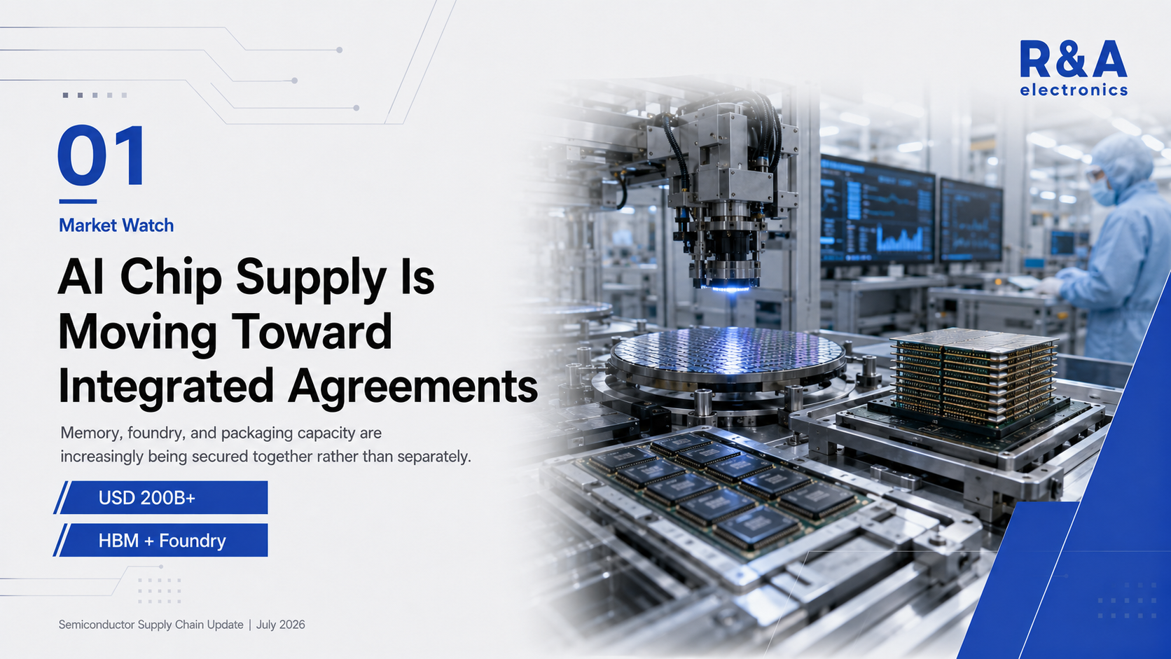
The semiconductor content required for AI infrastructure is becoming increasingly interconnected. AI accelerators depend on advanced logic, high-bandwidth memory, high-speed networking, power efficiency, thermal performance, and complex packaging technologies working together as one system.
This makes separate sourcing decisions more difficult. A company may secure sufficient logic wafer capacity but still face constraints in HBM supply or advanced packaging. It may also have access to memory and foundry capacity but encounter delays during integration, testing, or qualification.
By expanding cooperation across several production stages, Samsung and Broadcom are creating a more coordinated supply structure. This approach may improve visibility across product development, capacity planning, performance optimization, and long-term delivery schedules.
USD 200B+
Expected collaboration value across memory and foundry over five years through 2030.
2nm and Below
Samsung foundry technologies planned for Broadcom products and communications solutions.
HBM + Packaging
Collaboration includes HBM and advanced 2.3D and 2.5D integration technologies.
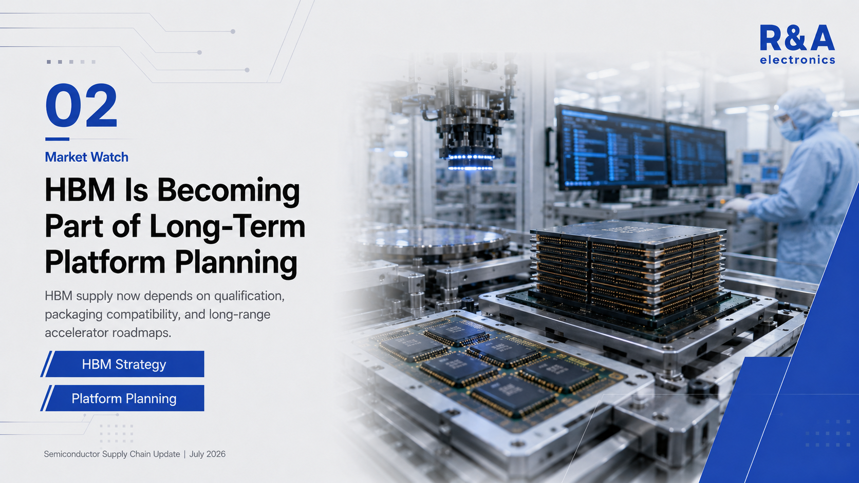
On the memory side, Samsung and Broadcom plan to pursue strategic cooperation for the supply of advanced memory solutions, including HBM, to support Broadcom’s next-generation AI accelerators.
HBM has become one of the most strategically important semiconductor categories in AI systems. Its supply is closely connected to accelerator design, advanced packaging, thermal performance, power consumption, and system-level bandwidth.
This means HBM purchasing cannot always be treated as a conventional memory procurement decision. Product specifications, qualification schedules, packaging compatibility, volume forecasts, and accelerator development timelines must be aligned much earlier.
Long-term cooperation may provide Broadcom with stronger visibility into future memory supply while giving Samsung clearer demand signals for capacity planning. The wider market implication is that future HBM availability may increasingly be shaped by strategic agreements with major AI customers.
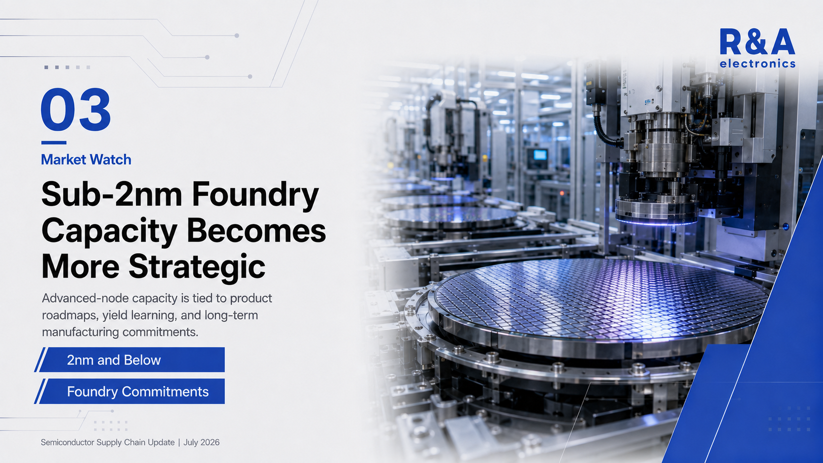
In foundry, the partnership focuses on Samsung’s 2-nanometer and below process technologies for Broadcom products, including Wireless Broadband Communications solutions.
The agreement gives Samsung an opportunity to strengthen utilization and customer commitments for its leading-edge manufacturing technologies. For Broadcom, it provides another advanced manufacturing route for high-performance AI and networking silicon.
This matters because advanced-node capacity is not interchangeable. Process design kits, IP libraries, performance targets, power requirements, yield development, and qualification schedules differ across foundries.
Once a product has been designed and qualified for a specific manufacturing route, moving it to another foundry may require substantial engineering work. Long-term foundry agreements therefore play an important role in both capacity security and product roadmap planning.
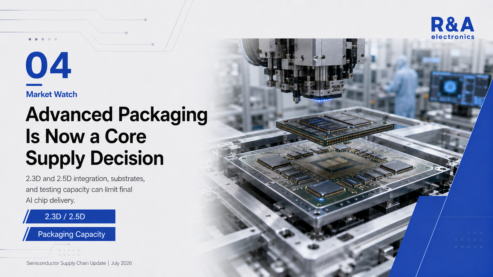
The partnership is also expected to extend to advanced packaging technologies based on Samsung’s 2nm process, including 2.3D and 2.5D integration.
Advanced packaging is increasingly central to AI semiconductor performance. It connects logic, memory, interposers, substrates, and other components into a single high-performance system while addressing bandwidth, power efficiency, and thermal requirements.
Packaging capacity can therefore become a production constraint even when logic wafers and memory devices are available. Integration complexity, substrate supply, thermal design, assembly yield, and testing capacity may all influence final delivery schedules.
By linking foundry and packaging cooperation, Samsung and Broadcom can coordinate manufacturing and integration more closely. The broader signal is that advanced packaging is no longer a downstream service added after chip production. It is becoming part of the original capacity and sourcing agreement.
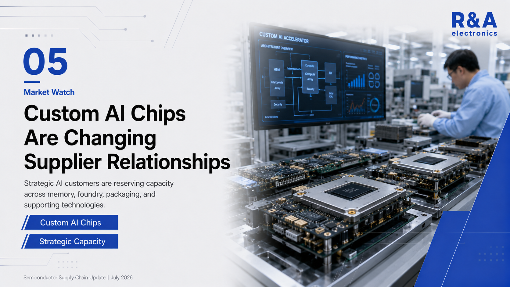
The Samsung–Broadcom agreement also reflects the growing importance of custom AI accelerators and application-specific integrated circuits.
As large technology companies develop more specialized AI processors, semiconductor suppliers must support increasingly customized requirements across memory bandwidth, process technology, power efficiency, networking performance, packaging architecture, and production scale.
These requirements encourage closer cooperation between chip designers and manufacturers. Instead of purchasing standard components from multiple independent sources, major AI customers may increasingly reserve capacity through strategic agreements covering several technologies.
This may create stronger supply assurance for strategic customers, but it may also reduce the amount of flexible capacity available to companies without similar long-term agreements.
Supply Competition May Shift From Components to Platforms
The agreement suggests that semiconductor supply competition is moving beyond individual products. The competitive unit is increasingly an integrated platform combining memory, logic manufacturing, packaging, connectivity, and engineering support.
This could benefit suppliers capable of offering several critical technologies within one manufacturing ecosystem. It may also encourage foundries, memory manufacturers, packaging providers, and chip designers to form deeper long-term partnerships.
For smaller customers and non-AI applications, the impact may be indirect. Capacity, engineering resources, supplier attention, and production priority may increasingly follow large strategic agreements, particularly in HBM, advanced logic, advanced packaging, and high-performance networking.
Procurement teams should therefore monitor not only market demand, but also which customers and suppliers are forming long-term capacity relationships across the semiconductor ecosystem.
What This Means for Procurement Teams
Procurement teams should view the Samsung–Broadcom partnership as a signal that semiconductor capacity is becoming more closely tied to strategic customer agreements. Availability may increasingly depend on long-term forecasting, qualification planning, and supplier relationships rather than short-term spot purchasing alone.
Procurement teams should monitor:
- Long-term capacity agreements
- HBM allocation and qualification schedules
- Advanced-node foundry commitments
- Advanced packaging availability
- Forecast submission requirements
- Single-foundry and single-package exposure
- Alternative manufacturing route readiness
Categories to review:
- Memory: HBM, advanced DRAM, high-performance memory solutions
- Foundry: 2nm and below process capacity, design qualification, IP readiness
- Packaging: 2.3D, 2.5D, interposers, substrates, assembly and testing
- AI silicon: custom accelerators, ASICs, networking and connectivity chips
- Supporting supply: power, thermal, optical and high-speed interface components
R&A View
The Samsung–Broadcom partnership is more than a large bilateral agreement. It reflects a broader shift in semiconductor sourcing from individual component transactions toward integrated, long-term capacity partnerships.
In AI infrastructure, memory, advanced logic, packaging, networking, power, and thermal performance are increasingly connected. Securing one category without visibility into the others may not be enough to protect a production schedule.
For procurement teams, the practical priority is to identify which components and manufacturing stages depend on limited capacity, long qualification cycles, or a small number of approved suppliers. Alternative sourcing should be reviewed before capacity becomes fully committed.
R&A Electronics will continue to monitor memory, foundry, packaging, and supporting component supply signals to help procurement teams respond to changes in semiconductor capacity and sourcing strategy.
Procurement teams should not only ask: "Is the chip available?" They should also ask: "Are the memory, foundry, packaging, and supporting capacity secured together?"
Frequently Asked Questions
Is the USD 200 billion figure a completed purchase order?
No. Samsung and Broadcom signed a memorandum of understanding, and the companies expect the collaboration across memory and foundry to exceed USD 200 billion over the next five years through 2030.
Which technologies are included in the partnership?
The announced scope includes advanced memory solutions such as HBM, Samsung’s 2nm and below foundry processes, and advanced packaging technologies including 2.3D and 2.5D integration.
Why is advanced packaging important to AI chips?
Advanced packaging integrates logic, memory, substrates, and other components into high-performance systems. It affects bandwidth, power efficiency, thermal performance, production yield, and final delivery schedules.
Does the agreement guarantee immediate production capacity?
Not necessarily. The announcement establishes a framework for expanded cooperation. Product development, qualification, capacity planning, production schedules, and commercial terms will still determine how the collaboration is implemented.
What should procurement teams do now?
Review exposure to HBM, advanced-node foundry capacity, packaging, substrates, and supporting components. Confirm qualification status, identify single-source dependencies, and evaluate alternative manufacturing routes before supply becomes more tightly committed.
Need support with semiconductor sourcing?
R&A Electronics helps procurement teams monitor memory, foundry, packaging, and component-level supply risks while reviewing sourcing options in a changing semiconductor market.
Contact R&A

